Introduction to Waveguide Writing
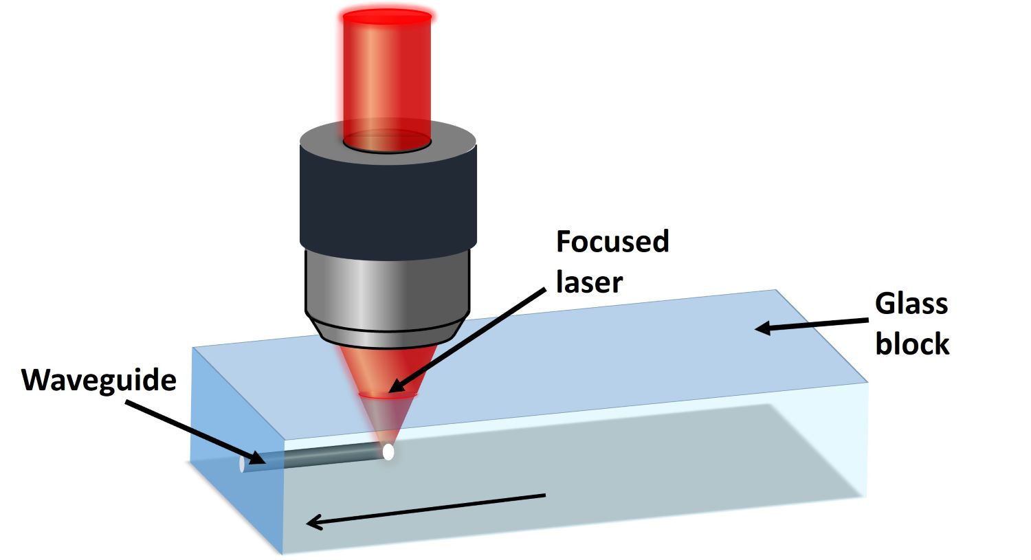
In order to write waveguides, we simply focus a laser into a transparent sample, such as glass. This creates a local change in the glass that has different optical properties (index of refraction) compared to the glass around it. When we then move the glass or the laser beam, we trace a path which becomes an optical “channel” or waveguide. This happens because the light (wave) is confined (guided) to the channel created by the path of the laser through the material (glass).

The focused laser beam moves through the glass block in the direction of the red arrow, tracing out the waveguide by changing the glass material as it goes.
Waveguide Writing Applications
In simple terms, waveguides can be used to move light from one place to another. They are not a one-size-fits-all solution and there are many ways to move light (e.g. via fibre, via ‘free-space’ i.e. sending the laser beam through air and others). Which method of transport the user chooses depends on the particular needs of the device or application they have, but in general, waveguides are often chosen when:
Overcoming The Space Constraints Of Fibres
A waveguide can be In the order of 10-20μm. While the core of a single mode fibre is ~9.5μm, the cladding on the fibre takes the size to 127μm or more. Waveguides can potentially be packed quite close together, but fibres are limited by the size of the cladding. The familiar example of this is in the area of chip-to-chip communication or transceiver applications, but other applications such as AR/VR/MR are emerging where space limitations are also driving the adoption of waveguides.
Efficient Compact Scale Connectivity
Since the glass connectors can be very small, propagation can be kept to a minimum. Waveguides written in glass suffer from relatively higher loss at 0.2dB/cm, while single mode fibres have losses of 0.2dB/km (note cm vs km!!)
Available on all devices
Capable of melee inscriptions
Suitable for coloured gemstones
High capacity (100k+ stones p/a)
Encryption secure IDs
Automation and machine vision
Remote service and diagnostics
Integrates with blockchain traceability solutions
Integrates with factory IM systems
Multiple stone loading
“The ability to write waveguide circuits through laser processing is a key enabler for a wide range of technological applications. Opsydia’s technology will be central to creating versatile devices on the industrial scale.”

Prof. Martin Booth
Founder & Director, Opsydia
Latest News
Opsydia at Laser World of Photonics 2025 in Munich
Opsydia attends the world’s leading trade fair in Munich in June 2025
Opsydia attended OFC 2025
Opsydia attended the OFC 2025 Conference from March 30-April 5, 2025 at the Moscone Center in San Francisco
Contact Us
To find out more about the Opsydia Systems or to discuss a trial or demonstration, please speak to a member of our team.


