Laser Assisted Chemical Etching for Semiconductor Interconnects (LACESI)
Artificial Intelligence (AI) and high-performance computing are driving exponential growth in bandwidth demand, exposing fundamental limitations in copper-based interconnects. At data rates above 200 Gbps, copper suffers from signal degradation, thermal inefficiency, and range limitations—creating a growing bottleneck for chip-to-chip communication. To address this, the semiconductor industry is exploring glass and other transparent materials as next-generation substrates for advanced packaging due to their mechanical stability, low coefficient of thermal expansion (CTE), and optical compatibility.
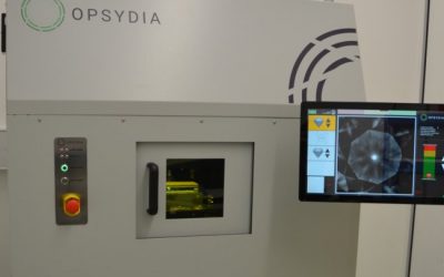
It is possible to form high-aspect-ratio, electrically conductive channels with arbitrary 3D geometry—referred to as non-line-of-sight (NLOS) vias – in transparent substrates such as glass, sapphire and others. Using Opsydia’s adaptive optic femtosecond laser writing, precursor tracks can be patterned with micron-scale accuracy, enabling the creation of vias that are curved, tapered, or blind—overcoming the geometric constraints of conventional vertical drilling.
Several important industry leaders such as Intel, Samsung and Corning are leading the way in the development of glass as a substrate material for interposers. There are many reasons for this including that glass is mechanically rigid, well behaved thermally and can be manufactured very cheaply.
Further Applications
It should be noted that glass is an electrical insulator and techniques to provide the electrical connections for a glass interposer are receiving a lot of attention. One approach of interest is Laser Induced Chemical Etching, wherein an ultrafast laser processes an area of glass, which is subsequently removed with a wet, alkaline etch and back filled with a metal to provide the electrical connections. As the Opsydia system could do the laser processing step directly, we are investigating this as an additional area for the company.
Available on all devices
Capable of melee inscriptions
Suitable for coloured gemstones
High capacity (100k+ stones p/a)
Encryption secure IDs
Automation and machine vision
Remote service and diagnostics
Integrates with blockchain traceability solutions
Integrates with factory IM systems
Multiple stone loading
Latest News
Opsydia secures breakthrough laser marking order from diamond giant De Beers
University of Oxford spinout Opsydia has secured the first order for its Opsydia D5000 Diamond Marking System. The sale, to industry giant De Beers for their Lightbox Jewelry business, follows over a year of development work and is a major step forward for Opsydia’s...
Laser marking by Oxford University spinout transforms diamond security
Opsydia, a spinout from the University of Oxford, has unveiled ground-breaking new technology that will help address the risk of tampering and counterfeiting in the diamond sector. Using high precision lasers, Opsydia can make tiny marks, less than 1/50th of the size...
Contact Us
To find out more about the Opsydia Systems or to discuss a trial or demonstration, please speak to a member of our team.