Diamond Devices & Nitrogen Vacancies
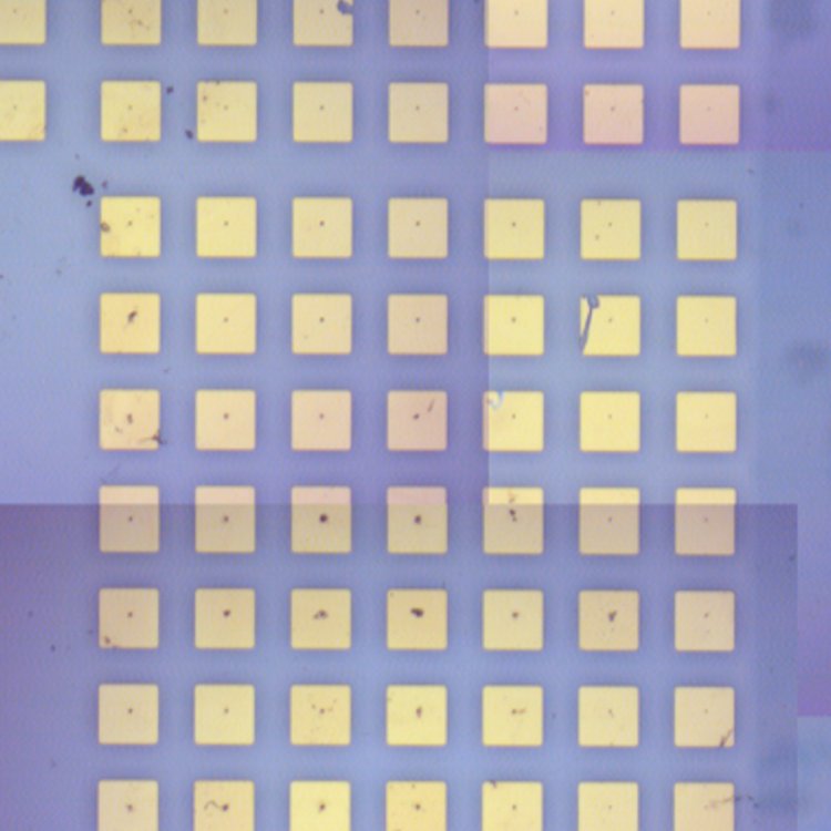
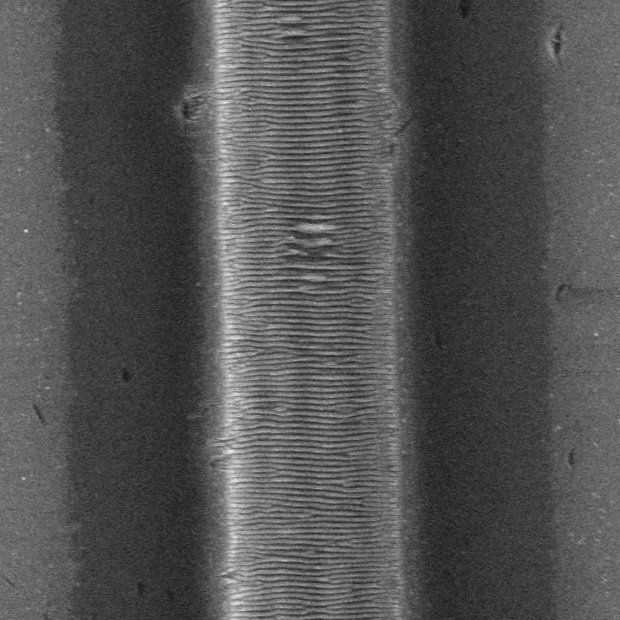
Opsydia technology provides a platform for next-generation functional devices in diamond. By modifying the diamond lattice, the laser process can be tailored to create optical or electrical responses. Nitrogen-vacancy centres and high spatial resolution conductive graphitic structures have been demonstrated in prototype devices and experiments. Currently in the research and development phase, the technology has a huge number of potential disruptive applications, from quantum devices to chemical and magnetic sensors.
What Are Nitrogen Vacancies?
Quantum Information systems can employ photonic components based on optically active point defects. One such defect is the nitrogen vacancy (NV) centre in diamond due to its potential for spin dependent photoluminescence with long coherence times. Other defects in diamond and other wide bandgap materials such as silicon carbide are also extremely interesting in this respect. However, the most challenging aspect of the manufacturing process remains the precise positioning of defect location. That can be achieved using Opsydia technology.
NV Centre Generation
Using Laser Writing
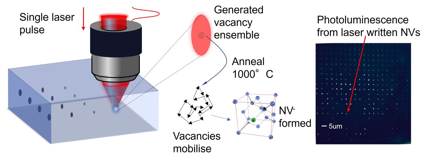
It is possible to create nitrogen vacancies with very high positional accuracy with adaptive optics direct laser writing techniques followed by appropriate annealing.

Laser processing is a powerful technique for fabrication of colour centre defects in diamond. A single ultrashort laser pulse generates an ensemble of vacancies in the diamond lattice. A subsequent thermal anneal mobilises the vacancies, so they can move in the lattice and become bound with pre-existing nitrogen atoms to form the famous nitrogen vacancy (NV) defect. The NV centres are detected via photoluminesence, which also reveals their quantum properties.
Example Applications
Quantum Information systems can employ photonic components based on optically active point defects. One class of such defects is the nitrogen vacancy (NV) due to its potential as a long lived light source in wide bandgap materials such as Silicon Carbide and Diamond. However, the most challenging aspect of the manufacturing process remains the precise place of defect location.
Radiation Detection
Electrically insulating, transparent and resilient, diamond is an ideal material for use in detection of high energy particles. Opsydia technology can create wide arrays of conductive electrodes inside diamond for high spatial resolution radiation detectors.
Chemical Analysis
As well as the world’s hardest material, diamond is extremely thermally conductive and almost entirely chemically inert. With tunable conductivity wires embedded into diamond sensor probes, chemical analysis can be performed in harsh environments.
Quantum Devices
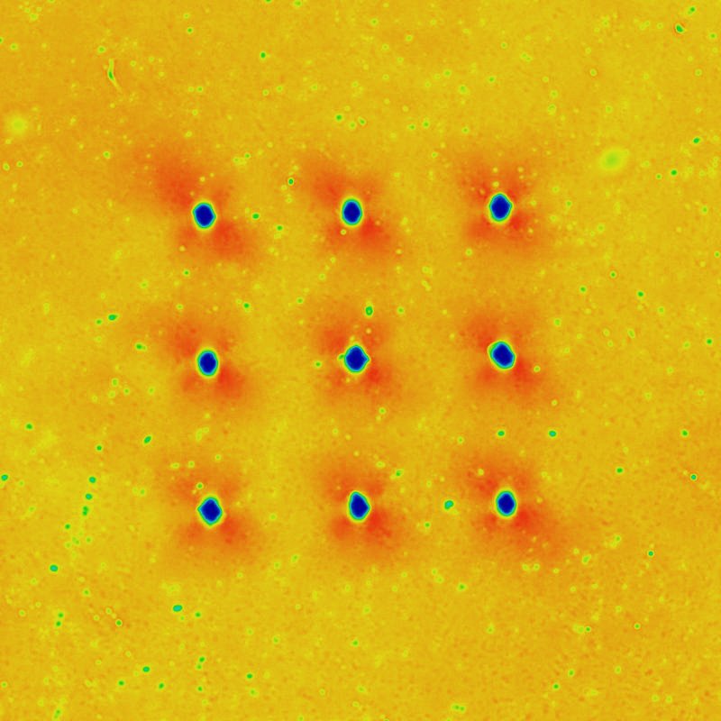
Diamond is one of the most exciting candidate materials for creating functional quantum information devices. Opsydia technology can create deterministic arrays of nitrogen-vacancy centres at high spatial resolutions.
Available on all devices
Capable of melee inscriptions
Suitable for coloured gemstones
High capacity (100k+ stones p/a)
Encryption secure IDs
Automation and machine vision
Remote service and diagnostics
Integrates with blockchain traceability solutions
Integrates with factory IM systems
Multiple stone loading
Contact Us
To find out more about the Opsydia Systems or to discuss a trial or demonstration, please speak to a member of our team.


